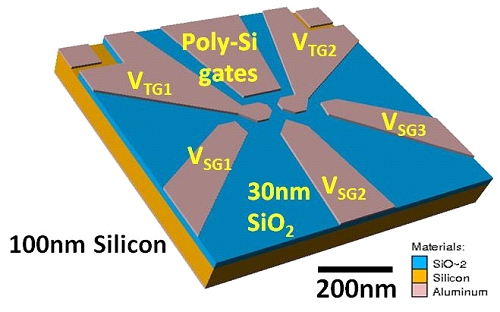
Silicon double quantum dots (DQD) structures have been an attractive candidate as an implementation of quantum bits. However, having larger effective mass compared to other common materials such as GaAs or Ge, requirements for silicon based DQD device are mostly difficult. The state of the art of the fabrication process for Silicon DQD is using MOS based structure, where quantum dots are defined electrostatically. However, this approach requires complicated process since multiple Electron Beam lithography with alignment is necessary.
This research intended to optimize the electrostatic approach in Silicon DQD fabrication. We propose a new approach in realizing silicon DQD, by designing a new simple device structure. The research comprise of two aspects. First, we simulate the device structure to find best structure for the DQD, with taking fabrication aspecst into account. Second, we optimize process and fabricate smallest quantum dots.Our simulation study has confirmed that formation of DQD structure and how the control of tunnel barrier are made possible in this device.
This research intended to optimize the electrostatic approach in Silicon DQD fabrication. We propose a new approach in realizing silicon DQD, by designing a new simple device structure. The research comprise of two aspects. First, we simulate the device structure to find best structure for the DQD, with taking fabrication aspecst into account. Second, we optimize process and fabricate smallest quantum dots.Our simulation study has confirmed that formation of DQD structure and how the control of tunnel barrier are made possible in this device.
